A few weeks ago, I found a great method for sending and receiving serial data.
When I did the UART lab in school we used cute com in order to send and receive a byte of information. for example, if I entered "Hello" in to the cute com, it would send something through the usb. The usb would enter the nexus 3 spartan6 board. some magic would happen and then it would send back the message through the usb and into the pc. then cutecom would show"Hello" again.
ie "HelloHello"
The problem was that I was using a mac and at the time I had no idea how to do something like cute com. I know about the existence of mini com but I did not want to download it. In the back of my mind I thought that this would be a great opportunity for me to make my own "mini com", but the question what how? I had many fruitless googling until I stumbled upon "screen".
Apparently "screen" could be used instead of "mini com" . This was great news! I'm not going to go into the technical details of how I interfaced my fpga with my mac book pro (10.7) because I had covered that in a past post.
Question....How to use screen? It isn't hard. After you plug it in you type this into the terminal without the quotes.
"screen <usbserial_com> <baud_rate>"
in my case the usbserial_com was "/dev/tty.usbserial-A700h2To"
and my baud rate "9600"
ie.
"screen /dev/tty.usbserial-A700h2To 9600"
How do I test if it works?
I pulled out one of my old UARTio labs from the past. All it did was receive and transmit. It was an unfinished project where I was suppose to add keyboard functionality to it, but I never got around to it. Luckly, my procrastination turned out for the better, cause now I could simply compile what I had without having to change anything.
I compiled it, and programmed the fpga. flipped the switches.
I ran the screen command that I mentioned above.
at first it looked like an empty terminal.
I typed "a" and I recieved an "a". I turned off the fpga and typed "a" again. nothing happened.
So the uartio was working correctly. I type something in, it goes to the fpga then pops back to the terminal. SWEET.
ok, what about a more realistic solution? eventually I would write a program that would read in an image (i.e. bmp) and send some info through the usb and write somewhere on the fpga memory.
So at first i thought I could write a c++ program that would run "screen"
But as it turns out, most programs wouldn't do that.
Eventually I found this neat site from arduino. It was meant for serial compunication with an arduino, but oh well, same difference.
http://todbot.com/arduino/host/arduino-serial/arduino-serial.c
Here is a link to more languages.
http://www.arduino.cc/playground/Main/InterfacingWithSoftware
As of now, I'm using the "C" version. Reason being that it is useful for osx/windows/linux.
The only problem is that I haven't quite figured out how it works. After tracing it with my eyes, I tried distilling the most essential parts so that I could make my own dedicated program. I failed. for now, But eventually I'll get it.
So then I tried using the Arduino C code as is and it actually worked.
ie ./a.out -b 9600 -p /dev/tty.usbserial-A700h2To -s 3; //actually sends the ascii version of 3.
Oh yeah, the data I send to the fpga shows up on the 8 led's so I can verify what is being sent.
TMR I will go through the program more carefully and trace its path. I WILL find out how to write my own.
Saturday, August 18, 2012
Friday, August 17, 2012
bram timing
I went ahead and played with Isim because I wanted to find out how long it would take for a value to be written to the bram data.
So I opened the ip generator and selected block ram.
16 wide and 16 tall.
I hooked up the DCM and tested it to see what would happen.
oh yeah, the DCM needs some special configurations. Instead of going blah blah, I'll just copy and past it right here
-------
DCM_CLKGEN_inst : DCM_CLKGEN
generic map (
CLKFXDV_DIVIDE => 2, -- CLKFXDV divide value (2, 4, 8, 16, 32)
CLKFX_DIVIDE => 1, -- Divide value - D - (1-256)
CLKFX_MD_MAX => 0.0, -- Specify maximum M/D ratio for timing anlysis
CLKFX_MULTIPLY => 256, -- Multiply value - M - (2-256)
CLKIN_PERIOD => 0.0, -- Input clock period specified in nS
SPREAD_SPECTRUM => "NONE", -- Spread Spectrum mode "NONE", "CENTER_LOW_SPREAD", "CENTER_HIGH_SPREAD",
-- "VIDEO_LINK_M0", "VIDEO_LINK_M1" or "VIDEO_LINK_M2"
STARTUP_WAIT => FALSE -- Delay config DONE until DCM_CLKGEN LOCKED (TRUE/FALSE)
)
port map (
CLKFX => CLKFX, -- 1-bit output: Generated clock output
CLKFX180 => CLKFX180, -- 1-bit output: Generated clock output 180 degree out of phase from CLKFX.
CLKFXDV => CLKFXDV, -- 1-bit output: Divided clock output
LOCKED => open, -- 1-bit output: Locked output
PROGDONE => open, -- 1-bit output: Active high output to indicate the successful re-programming
STATUS => open, -- 2-bit output: DCM_CLKGEN status
CLKIN => clock, -- 1-bit input: Input clock
FREEZEDCM => '0', -- 1-bit input: Prevents frequency adjustments to input clock
PROGCLK => open, -- 1-bit input: Clock input for M/D reconfiguration
PROGDATA => open, -- 1-bit input: Serial data input for M/D reconfiguration
PROGEN => open, -- 1-bit input: Active high program enable
RST => '0' -- 1-bit input: Reset input pin
);
-------
ok, to make a long story short, the multiplied clock signal shall be called "clkfx"
The not clock is called "clkfx180".
I write using the rising edge of clkfx180. I read using the rising edge of "clkfx"
This is mainly for the VGA screen. The timer needs to be in synce with read.
So anyways, how long DOES it take to write to the memory?
well, when I ramp the multiplier to 256, it takes 0.000144 us.
The down side was that clkfx must tick 5 times.
mult | time(ns) | clkfx ticks
256 | 0.144 | 5
128 | 0.183 | 3
64 | 0.183 | 2
32 | 0.339 | 2
16 | 0.724 |2
it seams like 64 multiplier seems to be the best choice. I just have to make sure that I hold the data value and the write enable needs to be held for 2 ticks.
lets say it takes 0.2 ns to write. How long will it take to clear the pixel mem?
The pixel mem has 320*240 = 76800 addresses.
0.2ns*76800 = 15360ns
--
perhaps I want the print to clear ratio to be 999:1
0.0153 sec or 15 ms will be spend printing .
this would have ~ 60hz period of writing and clearning.
Hopefully with this config, I would be able to get rid of the flicker the plagues my project.
-----
The duty is low, it shall work for the duration of 15360ns.
the duty will be high for the durations of 15 ms.
good exercices to do
This is for a computer architechture classes and I found their labs quite useful for practicing
http://students.cse.tamu.edu/wanglei/csce350/handout/lab6.html
http://students.cse.tamu.edu/wanglei/csce350/handout/lab6.html
Sunday, August 12, 2012
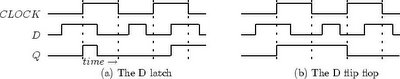
Latch verse flip-flop
It appears that in a latch, the clock is being used as an enable line which dictates WHEN D should set Q.
ie
Q <= D when enable = '1' else Q; --latch
It appears that a flip flop, uses the rising edge of the clock to write. D will set Q when it sees a rising edge.
ie
Q <= D when clock = '1' and clock'event else Q; --flip-flop
---------
The below is Reblogged from here
Many experienced engineers are clueless about the differences between a "Latch" and a "Flip Flop", and i have seen people using the terms synonymously. I feel that the right use of terminology is very critical in conveying the message more clearly.
I m sure the timing diagrams below is the best way of explanation.
ie
Q <= D when enable = '1' else Q; --latch
It appears that a flip flop, uses the rising edge of the clock to write. D will set Q when it sees a rising edge.
ie
Q <= D when clock = '1' and clock'event else Q; --flip-flop
---------
The below is Reblogged from here
I m sure the timing diagrams below is the best way of explanation.

Create logic gates out of muxes
I have created the AND, OR, NOT, gates using a multiplexer. With the power of these three you can make all the other logic gates.


Create 2x1 mux out of Nands
It appears to be possible to make a 2 by 1 mux out of NAND Gates.
In the picture below, I have two muxes. The one on top is a non-simplified version and the bottom is a minimized version. The non simplified version comes from simply swapping the AND and the OR gates into they NAND equivalents.

In the picture below, I have two muxes. The one on top is a non-simplified version and the bottom is a minimized version. The non simplified version comes from simply swapping the AND and the OR gates into they NAND equivalents.

Create all basic gates using NANDs
I've always known that you can use several NAND gates to create all the other gates, but never gave much thought as to how it would actually look like. Here is a picture that I exported from LogiSim. I created the logic in LogiSim to verify that it is equivalent.

begin
return (A NAND B)NAND(A NAND B);
end;
---
function "OR" (A,B:std_logic) return std_logic is
begin
return (A NAND A)NAND(B NAND B);
end;
---
function "NOT" (A:std_logic) return std_logic is
begin
return (A NAND A);
end;

---
VHDL
---
function "AND" (A,B:std_logic) return std_logic isbegin
return (A NAND B)NAND(A NAND B);
end;
---
function "OR" (A,B:std_logic) return std_logic is
begin
return (A NAND A)NAND(B NAND B);
end;
---
function "NOT" (A:std_logic) return std_logic is
begin
return (A NAND A);
end;
Subscribe to:
Posts (Atom)